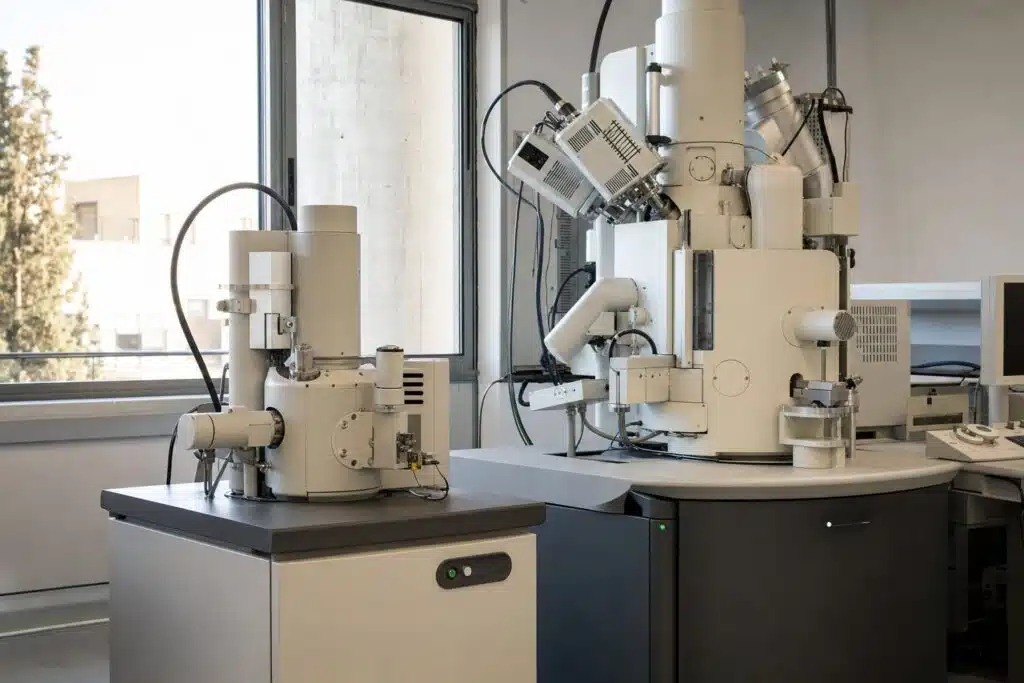
A field emission SEM (FESEM) uses a sharp emitter that produces a much brighter, narrower electron beam, giving finer resolution especially at low voltage, while a tungsten filament SEM is a lower-cost, robust workhorse for routine imaging. Both are scanning electron microscopes. They scan a focused beam over a sample and build an image from the electrons that come back. The difference is the electron source, and that one component shapes resolution, sample range, maintenance and price. This guide compares them with figures taken from the manufacturer pages on this site, so you can decide which suits your lab. For the technique itself, see our scanning electron microscope overview.
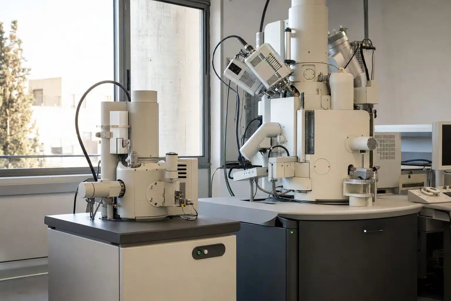
Table of Contents
What Is the Difference in Electron Source?
A tungsten filament is heated until it emits electrons thermally. It is simple, tolerant of poor vacuum and inexpensive to replace, but the emitting area is large, so the beam is less bright and the spot is larger. A field emission gun uses an extremely sharp tip and a strong electric field. A Schottky emitter, the common FESEM type, is heated and field assisted. It gives a much smaller source size, higher brightness and a longer lifetime, but needs ultra high vacuum. The Wikipedia article on the scanning electron microscope describes both sources.
Why brightness matters
A brighter source lets you form a small probe that still carries enough current. A smaller probe means finer detail, and enough current means a clean signal at fast scan speed.
How Do the Specifications Compare?
| Model | Source | Resolution | Voltage | Magnification |
|---|---|---|---|---|
| CIQTEK SEM2100 | Tungsten filament | 3 nm at 20 kV (SE) | 0.2 to 30 kV | 1x to 300,000x |
| CIQTEK SEM3200 | Tungsten filament | 3 nm at 30 kV (SE), 7 nm at 3 kV (SE) | up to 30 kV | 1x to 1,000,000x |
| CIQTEK SEM5000Pro (G2) | Schottky field emission | 0.7 nm at 15 kV, 1.1 nm at 1 kV | 0.02 to 30 kV | up to 2,500,000x |
The figures come from CIQTEK specifications. The largest gap appears at low voltage. The tungsten SEM3200 resolves 7 nm at 3 kV, while the Schottky SEM5000Pro reaches 1.1 nm at 1 kV, roughly a sixfold finer figure at a lower voltage.
Why Does Low Voltage Performance Matter?
Low accelerating voltage reduces beam penetration, so the signal comes from the top few nanometres of the sample. That shows true surface detail, and it reduces charging on insulating samples such as polymers, ceramics and biological material, often without a conductive coating. The SEM5000Pro uses in-lens beam deceleration with its Super Tunnel optics, which the manufacturer describes as a way to keep resolution at low landing energy.
What tungsten does well
A tungsten SEM at 15 to 30 kV is excellent for fractures, particles, cross sections and board-level inspection. The SEM3200 adds an optional low vacuum mode from 5 to 1000 Pa, which allows non-conductive samples to be examined without coating, and a five-axis motorized stage with 125 mm travel in X and Y. The SEM2100 keeps operation simple with automatic brightness, contrast, focus and stigmation.
Which Analytical Options Are Available?
Both families can be expanded. The SEM3200 lists backscatter detection, EDS or EDX, EBSD and a loadlock as options. The SEM5000Pro lists simultaneous in-lens, ETD and optional backscatter imaging, plus STEM, ECCI, EDS, EBSD and cathodoluminescence, and an optional 8 inch compatible loadlock. If you plan to add a focused ion beam later, our FIB-SEM guide explains the combination.
How Do You Prepare Samples for Either Type?
Samples must be dry, stable under vacuum and electrically grounded. Mount them on stubs with carbon tape or conductive paint, and blow off loose particles. Insulating samples can be coated with a few nanometres of gold, platinum or carbon, but coatings hide the finest surface detail, which is one reason low voltage imaging is attractive. Biological and wet samples need fixation and drying, or a low vacuum mode.
Choosing detector signals
Secondary electrons show topography and give the sharpest surface detail. Backscattered electrons show atomic number contrast, so heavier elements appear brighter. In-lens detectors on a field emission column collect secondary electrons efficiently at low voltage, which is why they pair well with beam deceleration.
Typical imaging workflow
Start at low magnification to find the area, set the working distance, then raise magnification while correcting focus and stigmation. Use the lowest beam current and voltage that still give a clean image, and take an image quickly if the sample is beam sensitive.
Which One Should You Choose?
- Choose a tungsten SEM for routine imaging, teaching labs, quality control and failure analysis where features are tens of nanometres or larger, and where budget and simple maintenance matter.
- Choose a field emission SEM for nanomaterials, thin films, semiconductor structures and any work needing a few nanometres of resolution or imaging at 1 kV and below.
- Consider both if demand is mixed. A tungsten SEM can carry the daily load while a shared FESEM handles the demanding projects.
Questions to ask a supplier
Ask which detectors are included, what the resolution is at the voltages you use most, what the vacuum requirements are, how long the emitter lasts and what the service plan covers. Ask for your own sample to be imaged during a demonstration, because brochure images are selected to look their best.
How Do Costs Compare Over Time?
The purchase price of a FESEM is higher than that of a tungsten SEM, and it also needs a better vacuum system and a stable room. In return, a Schottky emitter lasts far longer than a filament, so there are fewer replacements and less downtime. A tungsten filament is cheap but is a consumable, and a pre-aligned filament module, as the SEM2100 uses, makes the swap quick. Count service, consumables and training in the comparison, not only the list price.
Unsure whether you need a tungsten SEM or a field emission SEM?
Frequently Asked Questions
What is a field emission SEM?
It is a scanning electron microscope with a field emission electron gun, which gives a brighter and narrower beam than a tungsten filament and therefore finer resolution.
Is a FESEM better than a tungsten SEM?
For resolution, especially at low voltage, yes. For routine imaging, budget and simple upkeep, a tungsten SEM is often the better fit.
What resolution does a tungsten SEM reach?
The CIQTEK SEM2100 and SEM3200 are specified at 3 nm for secondary electrons at 20 kV and 30 kV respectively.
What resolution does a Schottky FESEM reach?
The CIQTEK SEM5000Pro (G2) is specified at 0.7 nm at 15 kV and 1.1 nm at 1 kV.
Can I image non-conductive samples?
Yes. Low voltage on a FESEM or an optional low vacuum mode on a tungsten SEM such as the SEM3200 reduces charging without a coating.
Which detectors can be added?
Options include backscatter detectors, EDS, EBSD and, on the SEM5000Pro, STEM and cathodoluminescence.
Last updated: November 2026